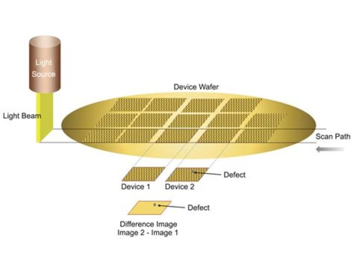
Wafer defect inspection system detects physical defects (foreign substances called particles) and pattern defects on wafers and obtains the position coordinates (X, Y) of the defects. Inspection can be performed on a patterned process wafer or on a bare wafer. Each of these has a different system configuration..
Hereof, what is a wafer used for?
In electronics, a wafer (also called a slice or substrate) is a thin slice of semiconductor, such as a crystalline silicon (c-Si), used for the fabrication of integrated circuits and, in photovoltaics, to manufacture solar cells. The wafer serves as the substrate for microelectronic devices built in and upon the wafer.
Subsequently, question is, how do you grow silicon wafers? To grow an ingot, the first step is to heat the silicon to 1420°C, above the melting point of silicon. Once the polycrystalline and dopant combination has been liquefied, a single silicon crystal, the seed, is positioned on top of the melt, barely touching the surface.
Also Know, what is wafer mapping?
Wafer mapping, or substrate mapping, is a process in which the performance of semiconductor devices on the surface of a substrate is visualized through the production of a color-coded grid.
What is semiconductor metrology?
Semiconductor metrology instruments are designed for wafer and thin film in-line inspection after semiconductor processing. By using semiconductor metrology instruments, manufacturers can facilitate semiconductor inspection, reduce manufacturing costs, and shorten the product development cycle.
Related Question Answers
How many chips are on a wafer?
Hmmm, this obviously depends on the size of the die (the silicon chips themselves). As a starting point, the area of a circle is Pi × r^2 (that's Pi times the radius of the circle squared). So if we have a 300 mm diameter wafer, its area will be 3.142 × 150^2 = 3.142 × 22,500 = 70,695 square millimeters.How much does a silicon wafer cost?
The retail price of a basic one-inch silicon wafer without any special features is about $21 when purchased in quantity. A bulk purchase of similar 6-inch silicon wafers costs about $125 per unit, which is about 6 times the price of the one-inch wafer.What is wafer made of?
Wafers are formed from flour and water dispersions (batter) with small amounts of fat, sugar, salt and sodium bicarbonate, which are mixed and then confined in preheated moulds3. Yeast may be used in place or in addition to sodium bicarbonate.How do you make a wafer from scratch?
To make the wafers: Beat 1/4 cup butter and sugar in medium bowl until light and fluffy. Beat in egg whites. Gradually mix in flour and salt (batter will be soft.) Drop batter by level teaspoonfuls onto prepared cookie sheets, spacing 3 inches apart.What is a wafer start?
Wafer Start means the initiation of Manufacturing Services with respect to a Prime Wafer. Wafer Start means the initial Wafer introduction to a process flow.WHAT IS wafer technology?
A wafer is a thin piece of semiconductor material, usually crystalline silicon, in the shape of a very thin disc that is used as a base for fabricating electronic integrated circuits (ICs) and silicon-based photovoltaic cells. A wafer is also known as a slice or substrate.How do you say Wafer?
Here are 4 tips that should help you perfect your pronunciation of 'wafers': - Break 'wafers' down into sounds: [WAY] + [FUHZ] - say it out loud and exaggerate the sounds until you can consistently produce them.
- Record yourself saying 'wafers' in full sentences, then watch yourself and listen.
Why are wafers circles?
One of the biggest reasons that wafers are round is because they are in that shape from the beginning. The silicon ingots that are used to grow the wafer are circular in shape. This is due to the process of dipping a seed crystal into molten silicon and rotating and slowly extracting as the crystal grows.How do you cut a wafer?
In the context of manufacturing integrated circuits, wafer dicing is the process by which die are separated from a wafer of semiconductor following the processing of the wafer. The dicing process can involve scribing and breaking, mechanical sawing (normally with a machine called a dicing saw) or laser cutting.How is a chip made?
The process of building transistors into a chip starts with a pure silicon wafer. It is then heated in a furnace to grow a thin layer of silicon dioxide on the top of the wafer. A light-sensitive photoresist polymer is then applied over the silicon dioxide.Does Silicon conduct heat?
Silicone has a low thermal conductivity, which means that it transfers heat at a low rate compared to other materials. In addition to simply resisting heat, silicone also exhibits thermal stability, or the ability to maintain its properties and structure over a wide temperature range.Why is epitaxial layer needed?
There are a number of reasons to use an epitaxial layer above the silicon: Better material - Even when you just want silicon, you can grow higher purity silicon by epitaxy than the silicon in the substrate. Epitaxy allows a lower doped layer to be grown on a higher doped layer.What is bumping in semiconductor?
Wafer bumping is an essential to flipchip or board level semiconductor packaging. Bumping is an advanced wafer level process technology where “bumps” or “balls” made of solder are formed on the wafers in a whole wafer form before the wafer is being diced into individual chips.Is silicon a crystal?
Crystalline silicon (c-Si) is the crystalline forms of silicon, either polycrystalline silicon (poly-Si, consisting of small crystals), or monocrystalline silicon (mono-Si, a continuous crystal). This silicon contains much lower impurity levels than those required for solar cells.What is silicon wafer preparation?
Chapter 4 - Silicon Wafers: Preparation and Properties. Wafers are cut from the ingot, shaped, polished, and cleaned to be ready for further processing or for device manufacturing. Silicon crystals or ingots grown with either CZ or FZ technique are typically up to 2 m in length.What is the mass of a silicon wafer?
Silicon for computer chips is grown in large cylinders called “boules” that are 300 mm in diameter and 2 m in length,as shown. (Figure 1) The density of silicon is 2.33 g/cm3. Silicon wafers for making integrated circuits are sliced from a 2.0 m boule and are typically 0.75 mm thick and 300.What are metrology tools?
Metrology provides the science, techniques, and precision measuring devices that are used to determine if parts or features of parts fit within the tolerances and dimensions specified for the part.What is inspection in metrology?
A Closer Look: Verifying Dimensional Accuracy. Dimensional Inspection, also called Dimensional Metrology, assesses the geometric characteristics of machined parts and products to verify their compliance with design specifications. Inspection is often a critical step during product development or following production.